| CPC H10B 51/30 (2023.02) [H10B 43/10 (2023.02); H10B 43/35 (2023.02)] | 9 Claims |
|
1. A nonvolatile memory device comprising:
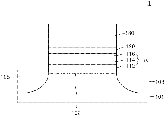
a substrate;
an electrode stack structure disposed on the substrate, wherein the electrode stack structure includes at least one gate electrode layer and at least one interlayer insulation layer alternatively stacked on the substrate;
a trench that penetrates the electrode stack structure and exposes sidewall surfaces of the gate electrode layer and the interlayer insulation layer;
an internal voltage amplification layer disposed to cover the interlayer insulation layer and the gate electrode layer along an inner surface of the trench, the internal voltage amplification layer being a ferroelectric layer having a negative capacitance;
a gate dielectric layer structure disposed on the internal voltage amplification layer, the gate dielectric layer structure having a positive capacitance; and
a channel layer disposed on the gate dielectric layer structure,
wherein the gate dielectric layer structure includes a charge tunneling layer, a charge trap layer and a charge barrier layer disposed on the channel layer,
wherein the nonvolatile memory device has an operation gate voltage corresponding to a polarization switching voltage of the internal voltage amplification layer,
wherein when the operation gate voltage is applied to the gate electrode layer, an internal voltage greater than the operation gate voltage is applied to the gate dielectric layer structure.
|