| CPC H10B 43/50 (2023.02) [H01L 23/535 (2013.01); H01L 25/0657 (2013.01); H10B 41/27 (2023.02); H10B 41/41 (2023.02); H10B 41/50 (2023.02); H10B 43/27 (2023.02); H10B 43/40 (2023.02); H01L 2225/0651 (2013.01); H01L 2225/06562 (2013.01); H01L 2225/06586 (2013.01)] | 20 Claims |
|
1. A semiconductor device comprising:
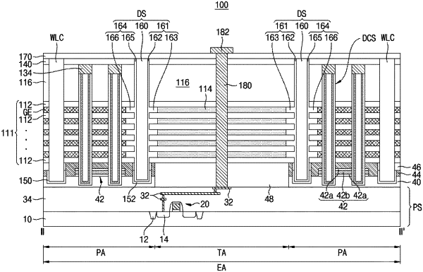
a substrate including a cell array area and an extension area, the extension area including a through electrode area;
a memory stack on the substrate and including gate electrodes, insulating layers and mold layers, the gate electrodes and the insulating layers being sequentially stacked, the mold layers including an insulating material and being disposed at the same levels as the gate electrodes in the through electrode area;
a channel structure extending vertically through the gate electrodes in the cell array area;
isolation insulating layers extending vertically through the memory stack and extending in a first horizontal direction parallel to the substrate, wherein the isolation insulating layers are spaced apart from one another in a second horizontal direction parallel to the substrate and intersecting with the first horizontal direction; and
a dam structure disposed between the isolation insulating layers and at least partially surrounding the through electrode area;
wherein the dam structure includes a dam insulating layer having a dam shape, an inner insulating layer disposed along an inner periphery of the through electrode area, and an outer insulating layer disposed along an outer periphery of the through electrode area, and
wherein the inner insulating layer includes first protrusions protruding in the first horizontal direction and arranged in a vertical direction perpendicular to the substrate, and the outer insulating layer includes second protrusions protruding in the first horizontal direction and arranged in the vertical direction.
|