| CPC H10B 43/27 (2023.02) [G11C 7/18 (2013.01); G11C 8/14 (2013.01); H01L 21/02019 (2013.01); H01L 21/67063 (2013.01); H01L 23/5226 (2013.01); H01L 29/0653 (2013.01); H10B 41/20 (2023.02); H10B 41/30 (2023.02); H10B 43/10 (2023.02); H10B 43/35 (2023.02); H10B 43/40 (2023.02); H01L 2221/1063 (2013.01)] | 8 Claims |
|
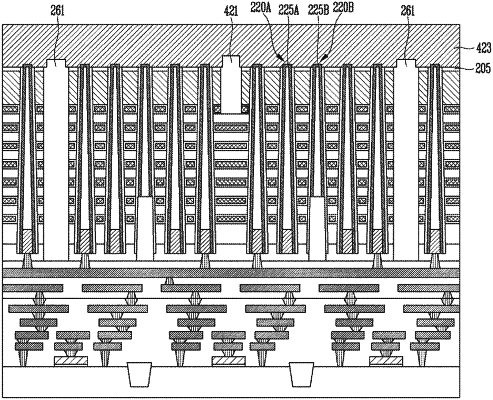
1. A method of manufacturing a semiconductor memory device, the method comprising:
forming a first select gate layer having a bottom surface facing a first substrate;
forming a stack structure, wherein the stack structure includes a second select gate layer overlapping with the first select gate layer and interlayer insulating layers and conductive patterns, which are alternately stacked on the second select gate layer;
removing the first substrate; and
etching the first select gate layer and the second select gate layer from the bottom surface of the first select gate layer to form a slit penetrating the first select gate layer and the second select gate layer.
|