| CPC H10B 43/27 (2023.02) [H10B 43/10 (2023.02); H10B 43/35 (2023.02)] | 9 Claims |
|
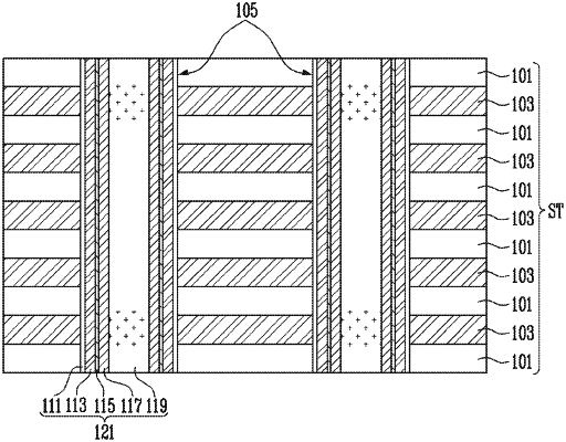
1. A semiconductor memory device comprising:
a stack with a plurality of interlayer insulating layers and a plurality of gate electrodes that are alternately stacked on a substrate; and
a plurality of channel structures passing through the stack in a vertical direction,
wherein each of the plurality of channel structures includes a core insulating layer, a channel layer, a tunnel insulating layer, and a charge storage layer that vertically extend in the same direction as the plurality of channel structures, and
wherein a dielectric constant of a first region of the core insulating layer, which corresponds to a source select transistor or a drain select transistor, is lower than a dielectric constant of a second region of the core insulating layer which corresponds to memory cells.
|