| CPC H10B 43/27 (2023.02) [H01L 23/5226 (2013.01); H10B 41/10 (2023.02); H10B 41/27 (2023.02); H10B 43/10 (2023.02); H10B 63/34 (2023.02); H10B 63/845 (2023.02)] | 16 Claims |
|
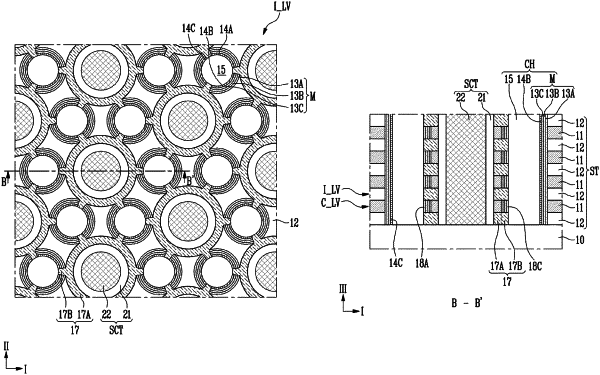
1. A semiconductor device, comprising:
a stacked structure with conductive layers and insulating layers that are stacked alternately with each other in a stacking direction;
an insulating pillar passing through the stacked structure;
a first channel pattern surrounding a sidewall of the insulating pillar;
a second channel pattern surrounding the sidewall of the insulating pillar;
first insulators located between the first channel pattern and the second channel pattern; and
a memory layer surrounding the first channel pattern, the second channel pattern, and each of the first insulators, the memory layer with a first opening that is located between the first channel pattern and the second channel pattern,
wherein the first insulators are separated from each other in the stacking direction.
|