| CPC H10B 43/10 (2023.02) [H01L 23/5226 (2013.01); H01L 23/5283 (2013.01); H10B 41/10 (2023.02); H10B 41/27 (2023.02); H10B 41/35 (2023.02); H10B 43/27 (2023.02); H10B 43/35 (2023.02)] | 20 Claims |
|
1. A semiconductor device comprising:
a lower structure;
a first main separation structure and a second main separation structure spaced apart from each other and on the lower structure;
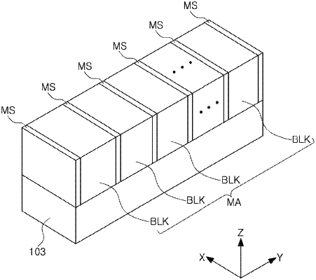
a stacked structure between the first main separation structure and the second main separation structure, and including a memory array region and an extended region;
vertical structures penetrating through the memory array region of the stacked structure;
first auxiliary separation structures penetrating through a first region of the extended region of the stacked structure, between the first main separation structure and the second main separation structure, and sequentially arranged in a first direction parallel to an upper surface of the lower structure; and
second auxiliary separation structures penetrating through a second region of the extended region of the stacked structure, between the first main separation structure and second main separation structure, and sequentially arranged in the first direction;
wherein each of the first and second auxiliary separation structures has a linear shape extending in a second direction perpendicular to the first direction,
wherein the stacked structure includes word lines and string selection lines on the word lines,
wherein a number of the string selection lines at a first height level is N,
wherein a number of the second auxiliary separation structures sequentially arranged in the first direction is N−2, and
wherein N is an integer greater than three (3).
|