| CPC H10B 12/34 (2023.02) [H01L 21/76224 (2013.01); H01L 21/76829 (2013.01); H01L 29/0653 (2013.01); H10B 12/053 (2023.02); H10B 12/315 (2023.02)] | 15 Claims |
|
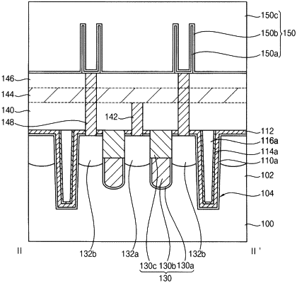
1. A method of manufacturing a semiconductor device, the method comprising:
etching a portion of a substrate to form an active pattern protruding from the substrate;
conformally forming a first silicon liner having a crystalline structure on surfaces of the active pattern and the substrate;
oxidizing a surface of the first silicon liner to form a second silicon liner and an insulation layer on the second silicon liner, the second silicon liner having a thickness less than a thickness of the first silicon liner, the second silicon liner and the insulation layer conformally along top and side surfaces of the active pattern;
forming an isolation layer on the insulation layer to fill a trench adjacent to the active pattern; and,
forming a transistor, the transistor including
a gate structure disposed on the second silicon liner, and
impurity regions, the impurity regions adjacent to respective sides of the gate structure.
|