| CPC H10B 12/315 (2023.02) [H10B 12/0335 (2023.02); H10B 12/053 (2023.02); H10B 12/09 (2023.02); H10B 12/34 (2023.02); H10B 12/50 (2023.02)] | 19 Claims |
|
1. A semiconductor memory device comprising:
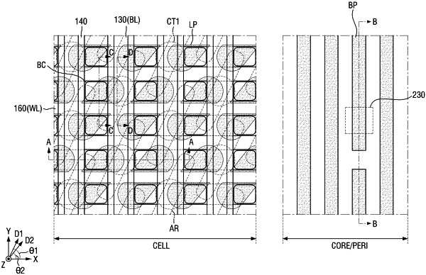
a substrate including an active region extending in a third direction;
a plurality of first conductive patterns extending parallel in a first direction different from the third direction on the substrate;
a plurality of second conductive patterns extending parallel in a second direction crossing the first direction on the substrate;
a plurality of buried contacts connected to the substrate between the plurality of first conductive patterns and between the plurality of second conductive patterns;
a landing pad on and connected to each of the plurality of buried contacts; and
a capacitor connected to the landing pad, and contacting a top surface of the landing pad,
the landing pad including a first side surface extending in the first direction in plan view and a second side surface extending in a fourth direction different from the first direction, the second direction, and the third direction in plan view,
the first side surface and the second side surface are not in direct contact with the capacitor,
the first direction, the second direction, the third direction, and the fourth direction being in a same plane, and
the third direction and the fourth direction are not perpendicular.
|