| CPC H10B 12/30 (2023.02) [H10B 12/03 (2023.02); H10B 12/05 (2023.02)] | 25 Claims |
|
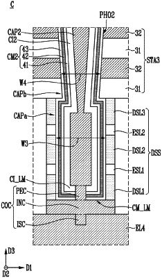
12. A semiconductor device, comprising:
a first stacked body comprising a first stacked insulating layer and a first stacked conductive layer that are alternately stacked;
a capacitor plug passing through the first stacked body;
a capacitor insulating layer configured to enclose the capacitor plug;
a capacitor multi-layered layer configured to enclose the capacitor insulating layer;
an electrode disposed under the capacitor plug; and
a connection conductor comprising a penetrating conductive part passing through the capacitor insulating layer and the capacitor multi-layered layer,
wherein the connection conductor is configured to couple the capacitor plug to the electrode.
|