| CPC H10B 12/30 (2023.02) [H01L 28/75 (2013.01)] | 20 Claims |
|
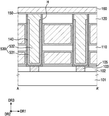
1. A semiconductor device comprising:
a substrate;
first and second supporter patterns stacked sequentially on the substrate in a first direction and spaced apart from an upper surface of the substrate;
a lower electrode hole that extends through the first and second supporter patterns on the substrate in the first direction;
an interface film on side walls and a bottom surface of the lower electrode hole;
a lower electrode inside the lower electrode hole on the interface film; and
a capacitor dielectric film that is in physical contact with side walls of the interface film, an uppermost surface of the interface film, and an uppermost surface of the lower electrode,
wherein the uppermost surface of the interface film is formed on a same plane as an upper surface of the second supporter pattern.
|