US 11,812,599 B2
Compute near memory with backend memory
Abhishek Sharma, Portland, OR (US); Noriyuki Sato, Hillsboro, OR (US); Sarah Atanasov, Beaverton, OR (US); Huseyin Ekin Sumbul, Portland, OR (US); Gregory K. Chen, Portland, OR (US); Phil Knag, Hillsboro, OR (US); Ram Krishnamurthy, Portland, OR (US); Hui Jae Yoo, Hillsboro, OR (US); and Van H. Le, Beaverton, OR (US)
Assigned to Intel Corporation, Santa Clara, CA (US)
Filed by Intel Corporation, Santa Clara, CA (US)
Filed on Feb. 11, 2022, as Appl. No. 17/670,248.
Application 17/670,248 is a division of application No. 16/827,542, filed on Mar. 23, 2020, granted, now 11,251,186.
Prior Publication US 2022/0165735 A1, May 26, 2022
Int. Cl. G11C 8/00 (2006.01); H10B 12/00 (2023.01); H01L 27/12 (2006.01); G11C 11/4096 (2006.01)
CPC H10B 12/00 (2023.02) [G11C 11/4096 (2013.01); H01L 27/124 (2013.01); H01L 27/1207 (2013.01); H01L 27/1225 (2013.01); H01L 27/1255 (2013.01); H01L 27/1266 (2013.01)] 18 Claims
OG exemplary drawing
 
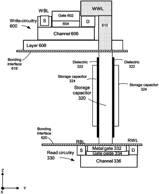
1. A method of forming a gain cell memory device comprising:
forming over a first substrate, a first region comprising a word line driver, a read circuitry, and active fins;
forming a dielectric region over the first region;
forming at least one storage region in the dielectric region;
forming a layer of at least one write circuit in contact with the at least one storage region;
bonding a structure onto a surface of the dielectric region; and
removing the first substrate to expose the active fins.