| CPC H10B 43/35 (2023.02) [H01L 23/5226 (2013.01); H10B 41/10 (2023.02); H10B 41/27 (2023.02); H10B 41/35 (2023.02); H10B 43/10 (2023.02); H10B 43/27 (2023.02)] | 14 Claims |
|
1. A three-dimensional memory device comprising:
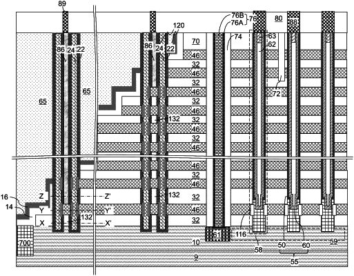
an alternating stack of insulating layers and electrically conductive layers and comprising stepped surfaces in a staircase region;
memory stack structures vertically extending through the alternating stack and comprising a respective vertical stack of memory elements located at levels of the electrically conductive layers;
a retro-stepped dielectric material portion overlying the stepped surfaces of the alternating stack;
a laterally perforated support pillar structure located in the staircase region and including an outer sidewall, an inner sidewall laterally offset inward from the outer sidewall, and lateral openings at levels of a subset of the electrically conductive layers, wherein each electrically conductive layer within the subset of the electrically conductive layers extends from outside of an area defined by the outer sidewall through the lateral openings into an area defined by the inner sidewall;
and a layer contact via structure laterally surrounded by the laterally perforated support pillar structure and contacting a top surface of a topmost electrically conductive layer of the subset of the electrically conductive layers.
|