| CPC H05K 5/0243 (2013.01) [B23B 27/20 (2013.01); G06F 1/1633 (2013.01)] | 3 Claims |
|
1. A case of an electronic device comprising:
an external case formed by processing an upper surface of a base of the case of the electronic device with a first head of a CNC device; and
at least one pattern formed by processing a side surface of the external case with a second head and a third head of the CNC device,
wherein the at least one pattern comprises a first pattern, a second pattern and a third pattern, and
wherein the first pattern is formed by processing on the side surface of the external case with the second head, and the second pattern and the third pattern are formed by processing on the first pattern with the third head,
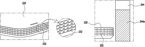
wherein the first pattern is formed of a transverse line shape on the side surface of the external case,
the second pattern is formed of a plurality of longitudinal line shapes crosses the transverse line shape of the first pattern on the side surface, and
the third pattern different from the second pattern is formed of a plurality of longitudinal line shapes crosses the transverse line shape of the first pattern on the side surface.
|