| CPC H05K 3/341 (2013.01) [B60R 1/04 (2013.01); B60R 1/12 (2013.01); B60R 16/023 (2013.01); H01R 9/0515 (2013.01); H01R 43/0256 (2013.01); H04N 7/10 (2013.01); H04N 7/181 (2013.01); H04N 23/51 (2023.01); H04N 23/54 (2023.01); H04N 23/55 (2023.01); H05K 1/111 (2013.01); H05K 1/181 (2013.01); H05K 3/0008 (2013.01); H05K 3/303 (2013.01); B60R 2001/1253 (2013.01); B60R 2300/105 (2013.01); B60Y 2410/10 (2013.01); B60Y 2410/115 (2013.01); H05K 2201/10121 (2013.01); H05K 2201/10151 (2013.01); H05K 2201/10189 (2013.01); H05K 2203/166 (2013.01); Y02P 70/50 (2015.11); Y10T 29/49117 (2015.01); Y10T 29/49124 (2015.01); Y10T 29/53174 (2015.01)] | 13 Claims |
|
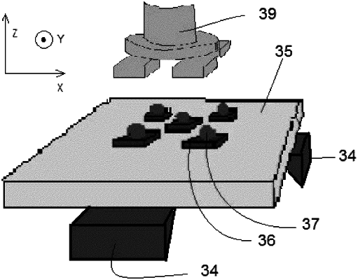
1. A method for assembling a camera suitable for use for a vision system of a vehicle, the method comprising:
providing a circuit board having first and second sides separated by a thickness dimension of the circuit board, wherein an imager is disposed at the first side of the circuit board, and wherein solder pads are disposed at the second side of the circuit board and in electrical connection with circuitry of the circuit board, and wherein each solder pad has solder paste disposed thereat;
aligning a coaxial connector at the solder pads at the second side of the circuit board;
soldering the coaxial connector at the second side of the circuit board via the solder pads, wherein soldering the coaxial connector at the second side of the circuit board comprises melting the solder paste at the solder pads;
providing a camera front housing and aligning a lens of the camera front housing with the imager and attaching the circuit board at the camera front housing; and
attaching a camera rear housing at the camera front housing to encase the circuit board, wherein the coaxial connector extends at least partially through a connector portion of the camera rear housing when the camera rear housing is attached at the camera front housing, and wherein the coaxial connector comprises a metallic material.
|