| CPC H05K 1/189 (2013.01) [H05K 1/118 (2013.01); H05K 1/186 (2013.01); H05K 3/284 (2013.01); H05K 3/32 (2013.01); A61B 2562/164 (2013.01)] | 21 Claims |
|
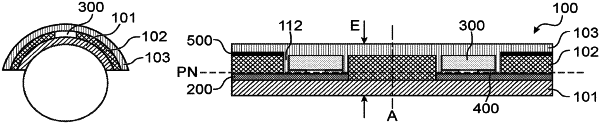
1. A flexible electronic structure comprising:
a first film, made of a first polymer or of glass,
a second film, made of a second polymer, wherein at least one electronic component is disposed, the second film covering the first film,
at least one electrically conductive track, disposed between the first film and the second film, and each electrically connected to one of the at least one electronic component, by a respective interconnection element, and
each interconnection element being disposed near a neutral plane of the structure, at a position through which a plane passes whose distance from the neutral plane is less than or equal to 20% of a total thickness of the structure,
wherein the structure further comprises at least one discontinuous compensation layer, formed of one or more discrete portions which each extend opposite one of the at least one electrically conductive track, respectively opposite one of the at least one electronic component,
wherein the neutral plane is located in the structure at a surface where compressive and tensile stresses compensate each other when the structure is subject to a bending process, and
wherein a respective metal via, electrically connected to one of the at least one electrically conductive track, extends in the first film so as to connect one of the at least one electronic component through the first film, the metal via being filled with the second polymer.
|