| CPC H05K 1/118 (2013.01) [H05K 1/189 (2013.01); H05K 2201/0979 (2013.01); H05K 2201/09445 (2013.01); H05K 2201/10674 (2013.01); H05K 2201/10734 (2013.01)] | 10 Claims |
|
1. A layout structure of flexible circuit board comprising:
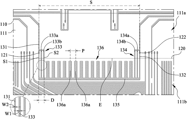
a flexible substrate including a top surface, a chip mounting area and a circuit area are defined on the top surface, and the circuit area surrounds the chip mounting area;
a chip mounted on the chip mounting area and including a first bump and a second bump, a space greater than 200 um exists between the first bump and the second bump, and there are no additional bumps disposed between the first bump and the second bump; and
a circuit layer including a first inner lead, a second inner lead, a first dummy lead, a second dummy lead, a transmission portion and a stress release portion, the first inner lead, the second inner lead, the first dummy lead and the second dummy lead are located on the chip mounting area, the first inner lead is electrically connected to the first bump, the first dummy lead is connected to the first inner lead and adjacent to the first bump, the second inner lead is electrically connected to the second bump, the second dummy lead is connected to the second inner lead and adjacent to the second bump, the transmission portion and the stress release portion are located on the circuit area, the transmission portion is electrically connected to the first inner lead and the second inner lead, the stress release portion is connected to the transmission portion and located between the transmission portion and an edge of the chip, wherein the stress release portion is a comb-shaped structure.
|