| CPC H05K 1/0298 (2013.01) [H05K 1/0218 (2013.01); H05K 1/0219 (2013.01); H05K 1/0222 (2013.01); H05K 1/0227 (2013.01); H05K 1/0221 (2013.01); H05K 2201/0715 (2013.01)] | 25 Claims |
|
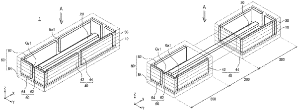
19. A printed circuit board, comprising:
a first insulating layer on which a wiring line is disposed;
a second insulating layer covering an upper portion of the wiring line;
a conductive shield wall disposed around the wiring line and spaced apart from the wiring line;
a flexible region in which the wiring line is disposed; and
a rigid region disposed on two opposing sides of the flexible region in a length direction of the wiring line, wherein the wiring line of the flexible region extends in the rigid region,
wherein the conductive shield wall comprises a plurality of via walls each being disposed in the rigid region and having a hexahedral shape, and
a portion of at least one of the first insulating layer or the second insulating layer is disposed in a gap between an adjacent pair of the plurality of via walls.
|