| CPC H05K 1/0242 (2013.01) [H05K 1/024 (2013.01); H05K 2201/0715 (2013.01); H05K 2201/09609 (2013.01); H05K 2201/09854 (2013.01)] | 13 Claims |
|
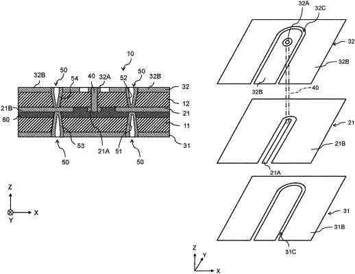
1. A high-frequency circuit comprising:
a first dielectric layer;
a circuit layer disposed on the first dielectric layer and including a transmission line of a high-frequency signal and a ground pattern disposed around the transmission line;
a second dielectric layer disposed such that the circuit layer is located between the first dielectric layer and the second dielectric layer; and
an electromagnetic wave shield disposed in the first dielectric layer and the second dielectric layer around the transmission line,
wherein the electromagnetic wave shield includes
a first ground electric conductor formed on an inner surface of at least one first hole formed to extend through the first dielectric layer without extending through the ground pattern,
a second ground electric conductor formed on an inner surface of at least one second hole formed to extend through the second dielectric layer without extending through the ground pattern, and
an adhesive disposed between the first dielectric layer and the circuit layer, the adhesive being also disposed between the transmission line included in the circuit layer and the ground pattern included in the circuit layer in plan view, and
the first ground electric conductor and the second ground electric conductor are each electrically connected to the ground pattern.
|