| CPC H05K 9/0045 (2013.01) [H05K 1/181 (2013.01); H05K 5/065 (2013.01)] | 3 Claims |
|
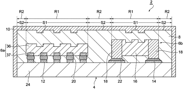
1. A circuit module comprising:
a wiring structure;
at least one electronic component arranged on an upper surface of the wiring structure;
an insulating resin layer provided on the upper surface of the wiring structure and in which the at least one electronic component is embedded; and
a metal layer provided on an upper surface of the insulating resin layer,
wherein when a surface roughness of a portion directly above the at least one electronic component on the upper surface of the insulating resin layer is expressed as R1, and a surface roughness of a portion other than the portion directly above the at least one electronic component on the upper surface of the insulating resin layer is expressed as R2, at least one R1 satisfies the condition: R1>R2,
when a surface roughness of a portion directly above the at least one electronic component on an upper surface of the metal layer is expressed as R3, at least one R1 and R3 satisfy the condition: R1>R3, and
at least a part of au upper surface of the at least one electronic component has a concave or a convex configuration, and
the upper surface of the insulating resin layer above the at least one electronic component and the upper surface of the at least one electronic component has a corresponding shape.
|