| CPC H04N 25/766 (2023.01) [H01L 27/1463 (2013.01); H01L 27/14614 (2013.01); H01L 27/14621 (2013.01); H01L 27/14627 (2013.01); H01L 27/14645 (2013.01); H04N 25/11 (2023.01); H04N 25/75 (2023.01); H04N 25/778 (2023.01); H04N 25/79 (2023.01)] | 20 Claims |
|
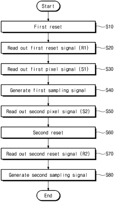
1. A method of operating an image sensor including a dual conversion gain transistor provided between and connected to a first charge detection node and a second charge detection node, and a reset transistor provided between and connected to the second charge detection node and a pixel power voltage, the method comprising:
performing a first reset operation to reset the first charge detection node and the second charge detection node;
turning off the dual conversion gain transistor and reading out a first reset signal from the first charge detection node;
transferring an electric charge accumulated in a photoelectric conversion device, to the first charge detection node and reading out a first pixel signal from the first charge detection node;
turning on the dual conversion gain transistor and reading out a second pixel signal from the first charge detection node;
performing a second reset operation to reset the first charge detection node and the second charge detection node; and
reading out a second reset signal from the first charge detection node.
|