| CPC H04N 25/705 (2023.01) [G01S 7/4863 (2013.01); G01S 17/894 (2020.01); H04N 25/75 (2023.01)] | 18 Claims |
|
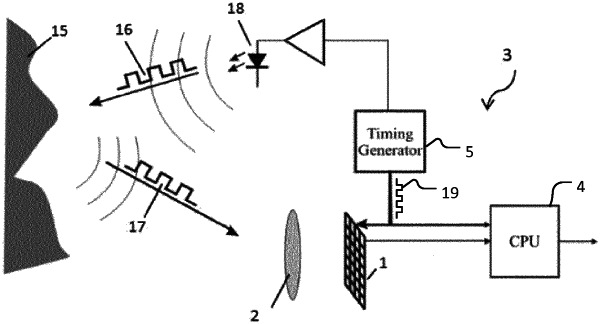
1. An electronic device comprising:
an array of pixels;
pixel modulation drivers, each pixel modulation driver being configured to drive a sub-array of the array of pixels, wherein the sub-array includes a group of pixels within the array of pixels, and wherein each pixel sub-array is configured to receive an individual demodulation signal and each pixel of a sub-array is configured to be controlled with an individual column enable control signal; and
switches connected to respective pixels of the array of pixels, each switch configured to be controlled by the respective individual column enable control signal and each switch configured to connect or disconnect the respective pixel to or from a respective pixel modulation driver.
|