| CPC H03K 5/1252 (2013.01) [H03K 17/16 (2013.01)] | 20 Claims |
|
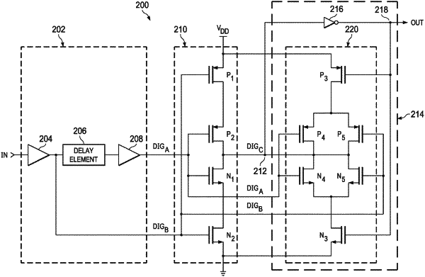
1. A glitch filter system comprising:
an input stage including a first output and a second output, the input stage including a delay element having an input and an output, the input being coupled to the first output of the input stage and the output being coupled to the second output of the input stage;
a C-element including a first input coupled to the first output of the input stage, wherein the C-element further includes a second input coupled to the second output of the input stage, and wherein the C-element further includes an output; and
an output latch including:
a first P-type transistor including a gate coupled to the second output of the input stage, wherein the first P-type transistor further includes a drain coupled to the output of the C-element, and wherein the first P-type transistor further includes a source;
a second P-type transistor including a gate coupled to the first output of the input stage, wherein the second P-type transistor further includes a drain coupled to the output of the C-element, and wherein the second P-type transistor further includes a source coupled to the source of the first P-type transistor;
a first N-type transistor including a gate coupled to the second output of the input stage, wherein the first N-type transistor further includes a drain coupled to the output of the C-element, and wherein the first N-type transistor further includes a source; and
a second N-type transistor including a gate coupled to the first output of the input stage, wherein the second N-type transistor further includes a drain coupled to the output of the C-element, and wherein the second N-type transistor further includes a source coupled to the source of the first N-type transistor.
|