| CPC H03H 9/13 (2013.01) [G06F 1/08 (2013.01); G06F 1/14 (2013.01); H03B 5/32 (2013.01); H03H 9/17 (2013.01)] | 6 Claims |
|
1. A real-time clock device comprising:
a resonator;
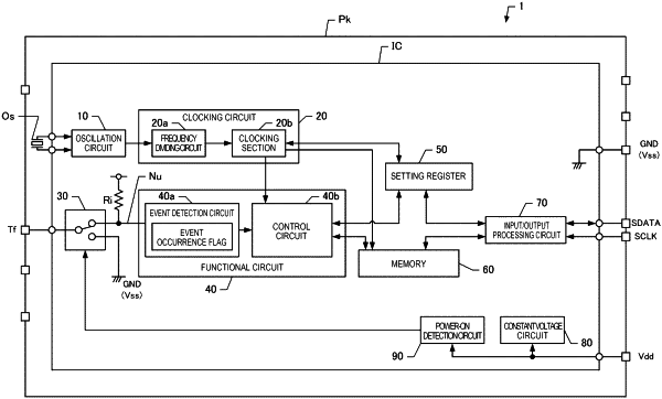
an oscillation circuit that oscillates the resonator;
a clocking circuit that performs clocking based on a signal from the oscillation circuit and generates clocking information;
a functional circuit that performs information processing based on the clocking information;
a package that houses the resonator, the oscillation circuit, the clocking circuit, and the functional circuit, the package being substantially quadrangular-prism-shaped, the package having a bottom outer surface having a first side, a second side, a third side, and a fourth side, the first and second sides extending in a first direction, the third and fourth sides extending in a second direction perpendicular to the first direction;
external terminals arranged on the bottom outer surface of the package along at least one of the first, second, third, and fourth sides; and
a switching circuit selectively electrically coupling one of the external terminals to the functional circuit,
wherein the external terminals include:
a high-potential power supply terminal coupled to a high-potential power supply;
a low-potential power supply terminal coupled to a low-potential power supply, a voltage supplied to the high-potential power supply terminal is higher than a voltage supplied to the low-potential power supply terminal;
a clocking signal terminal through which a clocking signal is transferred, and the clocking signal is used at least for controlling the clocking circuit; and
a functional signal terminal through which a functional signal is transferred via the switching circuit, and the functional signal is used for controlling the functional circuit,
the functional signal terminal is located at one of end areas of the first, second, third, and fourth sides on the bottom outer surface or one of four corners of the bottom outer surface of the package,
the high-potential power supply terminal, the low-potential power supply terminal, and the clocking signal terminal are located at an intermediate area between the end areas of at least one of the first, second, third, and fourth sides on the bottom outer surface of the package, and
the functional circuit is configured to output an interrupt signal to the functional signal terminal at a timing based on the clocking information.
|