| CPC H03H 9/02133 (2013.01) [H03H 3/02 (2013.01); H03H 9/02102 (2013.01); H03H 9/02125 (2013.01); H03H 9/0514 (2013.01); H03H 9/105 (2013.01); H03H 9/205 (2013.01); H03H 9/566 (2013.01); H10N 30/088 (2023.02); H03F 3/20 (2013.01); H03F 2200/451 (2013.01); H04B 1/3827 (2013.01)] | 20 Claims |
|
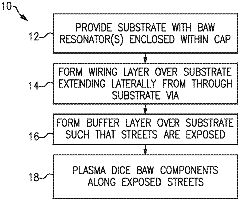
1. A bulk acoustic wave component comprising:
a substrate having a via extending therethrough;
at least one bulk acoustic wave resonator on the substrate;
a cap enclosing the at least one bulk acoustic wave resonator, the cap including a sidewall spaced apart from an edge of the substrate, the sidewall being 5 microns or less from the edge of the substrate; and
a conductor extending laterally from the via and electrically connected with a conductive layer in the via, the conductor being on an opposite side of the substrate than the at least one bulk acoustic wave resonator, the conductor having solder thereon, and the solder being non-overlapping with the via.
|