| CPC H03B 5/32 (2013.01) [H01L 23/5383 (2013.01); H01L 25/165 (2013.01); H01L 24/13 (2013.01); H01L 24/16 (2013.01); H01L 2224/13144 (2013.01); H01L 2224/16227 (2013.01)] | 10 Claims |
|
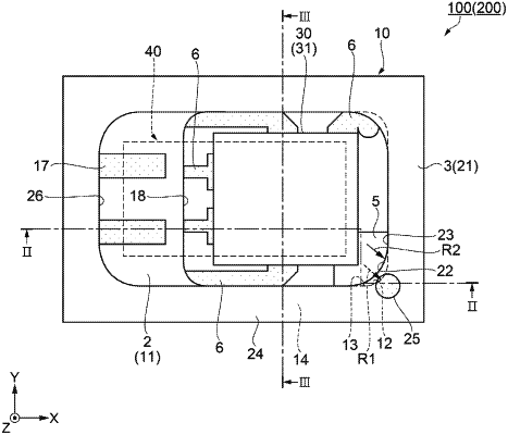
1. An electronic component package comprising:
a lid;
a first layer;
a second layer disposed between the first layer and the lid and configuring a first frame, the first frame having a first corner portion, the first corner portion having a first inner diameter R1 in a plan view;
a third layer disposed between the second layer and the lid and configuring a second frame the second frame having a second corner portion, the second corner portion having a second inner diameter R2 in the plan view, the first corner portion overlapping the second corner portion in the plan view;
a bonding member bonding the third layer to the lid; and
a via wire electrically coupled to the lid and penetrating the second frame, wherein
R1<R2, and
an inner surface of the second corner portion is located closer to a center of the electronic component package than an inner surface of the first corner portion and the via wire in the plan view.
|