| CPC H02M 7/5395 (2013.01) [H02M 1/34 (2013.01); H02M 1/344 (2021.05); H02M 1/348 (2021.05); H02M 5/42 (2013.01); H02M 7/12 (2013.01); H02M 5/453 (2013.01); H02M 5/458 (2013.01)] | 13 Claims |
|
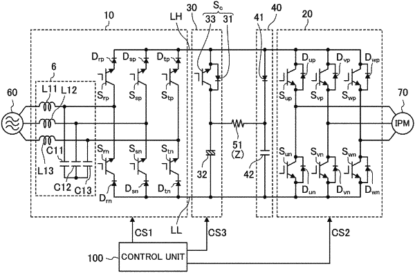
1. A power converter, comprising:
a converter circuit configured to generate from an AC voltage source a DC voltage with AC components superimposed;
an inverter circuit having an input connected with an output of the converter circuit, the inverter circuit being configured to
convert the DC voltage into an AC voltage by switching, and
output the AC voltage to an inductive load;
a clamp circuit including a first capacitor and a first diode connected in series, the clamp circuit being connected between a positive output and a negative output of the converter circuit;
a snubber circuit including a second capacitor and a second diode connected in series, the snubber circuit being connected between the positive output and the negative output of the converter circuit; and
an element including a resistive component,
a first output of the converter circuit, a second output of the clamp circuit, a third output of the snubber circuit, and the input of the inverter circuit being arranged in order,
the first and second diodes being connected on a positive side or a negative side with respect to the first and second capacitors,
the element being configured such that
the element connects between
a terminal of the first capacitor, the first diode being connected to the terminal of the first capacitor, and
a terminal of the second capacitor, the second diode being connected to the terminal of the second capacitor,
a first impedance from the positive output to the negative output being such that a second impedance across the clamp circuit is lower than a third impedance across the snubber circuit,
if the first and second diodes are connected on the positive side with respect to the first and second capacitors, a fourth impedance from a cathode of the second diode to the negative output are such that the second impedance across the clamp circuit is higher than the third impedance across the snubber circuit, and
if the first and second diodes are connected on the negative side with respect to the first and second capacitors, a fifth impedance from an anode of the second diode to the positive output are such that the second impedance across the clamp circuit is higher than the third impedance across the snubber circuit.
|