| CPC H02H 9/04 (2013.01) | 20 Claims |
|
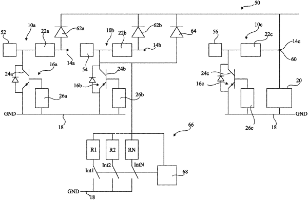
1. An electronic circuit comprising:
a plurality of first clipping circuits, each comprising:
a bipolar transistor, having a first conduction path coupled between a first node and a common second node; and
a second resistor coupled between a control terminal of the bipolar transistor and the common second node, wherein the second resistor is separate from the bipolar transistor;
a plurality of first resistors, each coupled between a respective one of the first nodes and a respective third node;
a second clipping circuit, shared by each of the first clipping circuits, and comprising a metal-oxide-semiconductor field-effect transistor having a second conduction path coupled between each third node and the common second node; and
a plurality of protected devices, each coupled to a respective one of the third nodes;
wherein at least one of the third nodes is coupled to a terminal of the second clipping circuit by a respective diode; and
wherein another one of the third nodes is connected to the terminal of the second clipping circuit without an intervening diode.
|