| CPC H02H 3/08 (2013.01) [H02H 1/0007 (2013.01); H02M 3/01 (2021.05)] | 7 Claims |
|
1. A compound control circuit, connected with a current detection port of a work control chip, the work control chip comparing a first electric signal received by the current detection port with an overcurrent protection level, the compound control circuit comprising:
an input end, connected with a detection point to obtain a second electric signal;
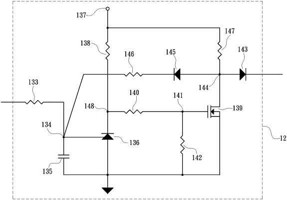
a light-load signal processing circuit, connected with the input end and receiving the second electric signal, the light-load signal processing circuit outputting a third electric signal based on a signal processing mechanism, the signal processing mechanism comprising two signal transition thresholds, and a potential of the third electric signal being determined based on the second electric signal and the two signal transition thresholds, wherein the light-load signal processing circuit comprises a sixth resistor, a fourth capacitor connected in series with the sixth resistor and forming a fifth node, a voltage stabilizing triode, a working voltage source, a seventh resistor connected with the working voltage source and the voltage stabilizing triode, a metal oxide semiconductor field effect transistor, an eighth resistor connected with the voltage stabilizing triode, a ninth resistor connected in series with the eighth resistor and forming a sixth node, a fifth diode connected with the slow response circuit and the fast response circuit, a sixth diode connected with the fifth diode and forming a seventh node, a tenth resistor connected in series with the sixth diode and connected with the fifth node, and an eleventh resistor connected with the working voltage source and the seventh node, a gate of the metal oxide semiconductor field effect transistor is connected with the sixth node, a drain electrode of the metal oxide semiconductor field effect transistor is connected with the seventh node, an anode of the fifth diode is connected with the seventh node, an anode of the sixth diode is connected with the seventh node, and the voltage stabilizing triode is connected with the seventh resistor and the eighth resistor to form an eighth node;
a slow response circuit, receiving the second electric signal and the third electric signal from the input end and the light-load signal processing circuit, the slow response circuit storing energy with the second electric signal and the third electric signal, if the energy stored by the slow response circuit reaches a first response threshold, the first electric signal with a potential corresponding to the overcurrent protection level being provided to the current detection port; and
a fast response circuit, receiving the second electric signal and the third electric signal from the input end and the light-load signal processing circuit, and if a potential of the second electric signal and the potential of the third electric signal are accumulated to reach a second response threshold, the fast response circuit quickly providing the first electric signal with the potential corresponding to the overcurrent protection level to the current detection port threshold.
|