| CPC H02G 3/16 (2013.01) [H01R 4/38 (2013.01); H01R 4/58 (2013.01)] | 4 Claims |
|
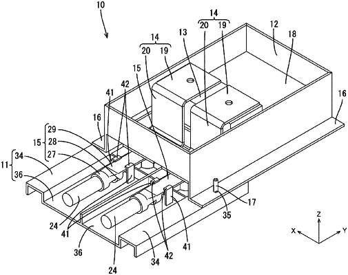
1. A circuit structure comprising:
an upper case having positioning holes;
a bus bar that is provided in a device disposed in the upper case and that has a through hole;
a terminal that is connected to an electric wire and that has a bolt disposed thereon that penetrates the through hole;
a nut that sandwiches the bus bar between the nut and the terminal by being screwed onto the bolt; and
a lower case that is attached to the upper case,
wherein the lower case includes: a terminal positioning portion that projects upward from the lower case and positions the terminal relative to the lower case by coming into contact with the terminal; and case positioning portions that project upward from the lower case and that are inserted into the positioning holes.
|