| CPC H01S 5/024 (2013.01) [H01S 5/02415 (2013.01); H01S 5/02469 (2013.01)] | 14 Claims |
|
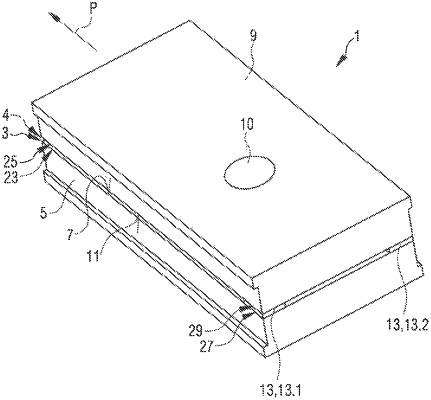
1. A diode laser arrangement, comprising:
a diode laser device having a first diode main surface and a second diode main surface;
a first cooling element having a first outer surface with a first front region;
a second cooling element having a second outer surface with a second front region;
at least one spacing device;
said diode laser device and said at least one spacing device being mutually spaced apart between said first cooling element and said second cooling element;
said diode laser device and said at least one spacing device being disposed on said first outer surface and on said second outer surface;
said first cooling element and said second cooling element being configured to cool said diode laser device;
said diode laser device having at least one of said first diode main surface disposed on said first front region of said first outer surface or said second diode main surface disposed on said second front region of said second outer surface;
said at least one spacing device configured to orient said first cooling element and said second cooling element relative to one another to place at least one of said first front region of said first outer surface parallel to said first diode main surface or said second front region of said second outer surface parallel to said second diode main surface;
said at least one spacing device having a first contact surface disposed on said first outer surface and a second contact surface disposed on said second outer surface; and
at least one of said first contact surface being smaller than 1/10 of said first diode main surface or said second contact surface being smaller than 1/10 of said second diode main surface.
|