| CPC H01S 5/02345 (2021.01) [H01S 5/0239 (2021.01); H01S 5/0261 (2013.01)] | 8 Claims |
|
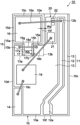
1. An optical semiconductor device comprising:
a semiconductor laser chip;
an insulation substrate having a surface mounting the semiconductor laser chip thereon;
a ground pattern provided on the surface;
a mounted pattern provided on the surface, the mounted pattern having an opposite side opposite to the ground pattern;
a resistor disposed such that a side edge of the resistor separates from an extension region of the opposite side;
an extension ground pattern positioned in the extension region of the opposite side, the extension ground pattern being electrically connected to the ground pattern; and
a capacitor disposed on the mounted pattern,
wherein the extension ground pattern is a pair of extension ground patterns, and the pair of extension ground patterns sandwich the resistor therebetween.
|