| CPC H01R 4/187 (2013.01) [H01L 23/49811 (2013.01); H01R 12/58 (2013.01)] | 18 Claims |
|
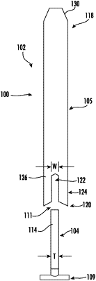
10. An electrical contact, comprising:
a first component including a base slot defined by a first set of prongs, the first component coupleable with a substrate; and
a second component including an upper slot defined by a second set of prongs, wherein the first set of prongs engage the second set of prongs when the first component and the second component are coupled together,
wherein the base slot is further defined by a first base wall, wherein the upper slot is further defined by a second base wall, wherein the first base wall and the second base wall engage one another when the first component and the second component are coupled together, wherein the first set of prongs and the second set of prongs are oriented parallel to a lengthwise axis extending through the first component and the second component, and wherein the lengthwise axis is perpendicular to a plane defined by an upper surface of the substrate.
|