| CPC H01L 33/62 (2013.01) [H01L 25/0753 (2013.01); H01L 25/167 (2013.01); H01L 27/1259 (2013.01); H01L 33/38 (2013.01); H01L 33/24 (2013.01); H01L 33/60 (2013.01); H01L 2933/0016 (2013.01); H01L 2933/0066 (2013.01)] | 18 Claims |
|
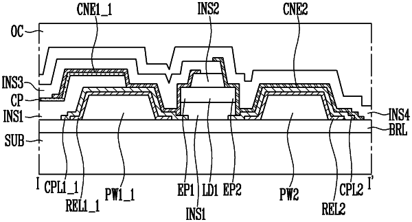
1. A light emitting device comprising:
a substrate comprising a plurality of unit light emitting regions; and
a pixel disposed in each of the plurality of unit light emitting regions,
wherein the pixel comprises:
a first wall and a second wall disposed on the substrate, the first wall and the second wall being spaced apart from each other;
a first electrode disposed on the first wall, and a second electrode disposed on the second wall and being spaced apart from the first electrode;
a first insulating layer disposed on the first electrode and the second electrode;
a light emitting element disposed on the first insulating layer, the light emitting element comprising a first end portion and a second end portion;
a first contact electrode disposed on the first end portion of the light emitting element and the first electrode, the first contact electrode connecting the first electrode and the first end portion of the light emitting element;
a second contact electrode disposed on the second end portion of the light emitting element and the second electrode, the second contact electrode connecting the second electrode and the second end portion of the light element; and
an overcoat layer disposed on the second contact electrode.
|