| CPC H01L 33/62 (2013.01) [H01L 27/156 (2013.01); H01L 33/382 (2013.01)] | 7 Claims |
|
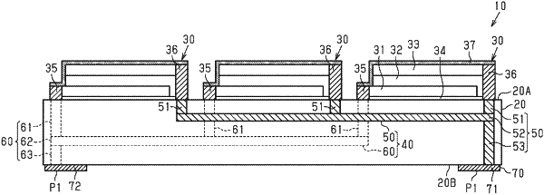
1. A light-emitting device, comprising:
a ceramic substrate;
a light-emitting element formed on an upper surface of the ceramic substrate; and
a wiring arranged inside the ceramic substrate and electrically and directly connected to the light-emitting element,
wherein the light-emitting element includes a structure in which a lower semiconductor layer, an active layer, and an upper semiconductor layer are sequentially stacked;
the light-emitting element is one of a plurality of light-emitting elements formed on the upper surface of the ceramic substrate;
the plurality of light-emitting elements are electrically and directly connected to the wiring;
each of the plurality of light-emitting elements includes:
a first electrode formed on the upper surface of the ceramic substrate and connected to the lower semiconductor layer, and
a second electrode formed on the upper surface of the ceramic substrate and connected to the upper semiconductor layer;
the first electrode and the second electrode are electrically and directly connected to the wiring, and
the first electrode of one of two adjacent ones of the plurality of light-emitting elements is connected to the first electrode or the second electrode of the other one of the two adjacent ones of the plurality of light-emitting elements.
|