| CPC H01L 31/0725 (2013.01) [H01L 31/0323 (2013.01); H01L 31/028 (2013.01); H01L 31/02725 (2013.01); H01L 33/343 (2013.01)] | 15 Claims |
|
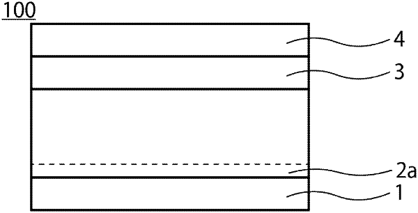
1. A solar cell comprising:
a p-electrode;
a p-type light-absorbing layer directly in contact with the p-electrode;
an n-type layer; and
an n-electrode, wherein
the n-type layer is disposed between the p-type light-absorbing layer and the n-electrode, and
a region in the p-type light absorbing layer from an interface between the p-type light-absorbing layer and the p-electrode toward the n-type layer is a p+ type region including a p-type dopant with a depth of 30 nm to 70 nm,
wherein the p-type light-absorbing layer is a semiconductor layer made of an oxide of metal containing Cu,
a maximum concentration of the p-type dopant in the p+ type region is 5.0×10¹⁹ atoms/cm3 or more and 1.0×10²¹ atoms/cm3 or less,
an average concentration of the p-type dopant in the p+ type region is 1.0×10¹⁹ atoms/cm3 or more and 1.0×10²⁰ atoms/cm3 or less; and
the p-type dopant includes Si.
|