| CPC H01L 31/035281 (2013.01) [H01L 31/028 (2013.01); H01L 31/02327 (2013.01); H01L 31/103 (2013.01); H01L 31/1804 (2013.01); H01L 31/1872 (2013.01)] | 20 Claims |
|
1. A photodetector, comprising:
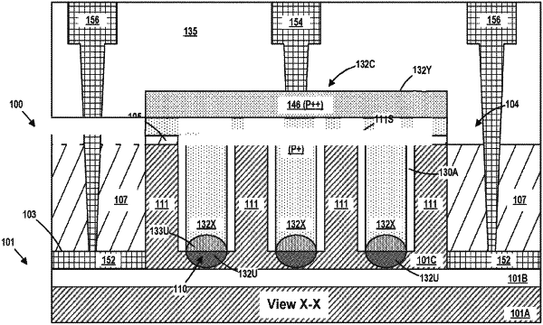
a waveguide structure defined in a semiconductor material, the waveguide structure comprising a plurality of first fins, wherein each adjacent pair of the plurality of first fins is separated by a trench;
a detector structure positioned on the waveguide structure, wherein a portion of the detector structure is positioned laterally between the plurality of first fins, wherein the detector structure comprises a single crystal semiconductor material;
a diffusion region that extends from a bottom surface of the trench into the semiconductor material, wherein the diffusion region comprises atoms of the single crystal semiconductor material of the detector structure;
at least one contact region positioned in the semiconductor material; and
a contact region positioned in the detector structure.
|