| CPC H01L 31/035236 (2013.01) [H01L 31/03046 (2013.01)] | 2 Claims |
|
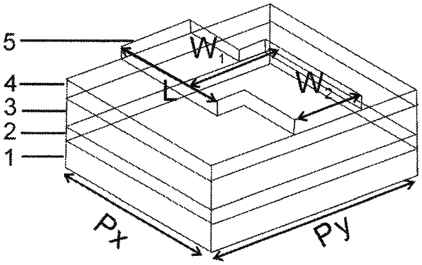
1. An integrated infrared circular polarization detector, wherein
the detector structurally comprises a bottom metal reflective surface (1), a bottom electrode layer (2), a quantum well layer (3), a top electrode layer (4) and a two-dimensional chiral metamaterial layer (5) in sequence from bottom to top, the two-dimensional chiral metamaterial layer (5) is comprised of Z-shaped antenna structures arranged periodically in an x-direction and a y-direction, so as to excite a surface plasmon polariton wave upon receiving circularly polarized light with selected handedness and not excite the surface plasmon polariton wave upon receiving circularly polarized light with opposite handedness;
the bottom metal reflective plane (1) is a metal reflective layer with a thickness of h1 which is not less than twice the skin depth of an electromagnetic wave in the metal reflective layer; and the metal reflective plane (1) is made of a highly conductive metal;
the bottom electrode layer (2) and the top electrode layer (4) are GaAs heavily doped with silicon at a doping concentration of 2×1017 cm−3; and
the quantum well layer (3) is made of a single-stack or a multi-stack semiconductor quantum well composed of GaAs/AlxGa1-xAs or InGaAs/GaAs.
|