| CPC H01L 29/7883 (2013.01) [H01L 29/1083 (2013.01); H01L 29/161 (2013.01); H01L 29/66825 (2013.01)] | 21 Claims |
|
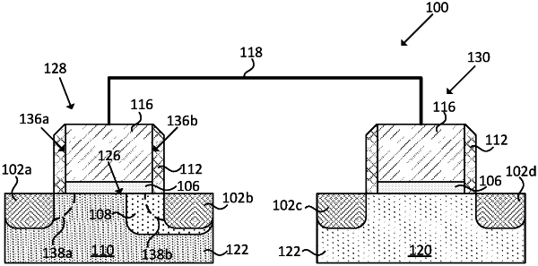
1. A nonvolatile memory device comprising:
a floating gate over a first p-well in a substrate;
an n-doped source, an n-doped drain, and a doped region in the first p-well, wherein the doped region is at least partially under the floating gate and adjacent to one of the source and the drain and spaced from the other of the source and the drain; and
halo regions adjacent to the source and the drain, wherein the doped region overlaps one of the halo regions adjacent to the source and the drain.
|