| CPC H01L 29/7824 (2013.01) [H01L 21/761 (2013.01); H01L 29/063 (2013.01); H01L 29/0649 (2013.01); H01L 29/1095 (2013.01); H01L 29/66681 (2013.01)] | 20 Claims |
|
1. A semiconductor device having a transistor comprising:
a semiconductor substrate;
an insulator on the semiconductor substrate;
an epitaxial layer of a first conductivity type and a first active doping concentration formed on the insulator, the epitaxial layer having a surface that is opposite to the insulator;
a source region of a second conductivity type within the epitaxial layer;
a channel region adjacent the source region;
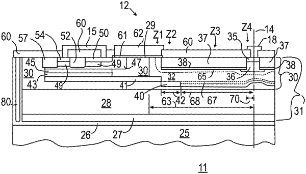
a drift region of the second conductivity type formed within the epitaxial layer, the drift region extending laterally to the channel region and having a notch extending a first distance from the surface of the epitaxial layer into the drift region, the notch having a bottom surface extending laterally across the notch;
an accumulation region of the second conductivity type formed as a first zone of the drift region adjacent to a first edge of the notch, the accumulation region having a first width and extending a first depth into the drift region and having a first bottom, the first zone having a second active doping concentration of the second conductivity type adjacent the surface, and a third active doping concentration extending vertically from the second active doping concentration to the first bottom wherein the third active doping concentration is substantially constant and is lower than the second active doping concentration;
a first counter-doped region abutting the first bottom and positioned between the first bottom and the epitaxial layer, the first counter-doped region having the first conductivity type and a fourth active doping concentration that is greater than the first active doping concentration wherein a first P-N junction is formed along an interface with the first bottom;
a second zone of the drift region formed underlying a first portion of the notch and abutting the first zone, the second zone having a second width extending laterally across the drift region from under the first edge of the notch and extending a second depth from the bottom surface of the notch into the drift region wherein the second depth is greater than the first depth and wherein the second zone has a second bottom, the second zone having substantially the second active doping concentration of the second conductivity type a first distance from the bottom surface of the notch, and substantially the third active doping concentration extending vertically from the first distance to the second bottom;
a second counter-doped region abutting the second bottom and positioned between the second bottom and the epitaxial layer, the second counter-doped region having the first conductivity type and substantially the fourth active doping concentration wherein a second P-N junction is formed along an interface with the second bottom;
a third zone of the drift region formed abutting the second zone and underlying a second portion of the notch that is adjacent to the first portion of the notch, the third zone extending laterally across the drift region a third width from the second zone and a third depth from the bottom surface of the notch into the drift region wherein the third depth is greater than the second depth, the third zone having a third bottom abutting a portion of the epitaxial layer, the third zone having substantially the second active doping concentration of the second conductivity type substantially the first distance from the bottom surface of the notch, a fifth active doping concentration extending a second distance from the third bottom toward the bottom surface of the notch wherein the fifth active doping concentration is substantially the same as the second active doping concentration, the third zone having substantially the third active doping concentration of the second conductivity type within the third zone that is positioned deeper than the third depth and more than the second distance from the third bottom; and
a fourth zone of the drift region formed within the drift region adjacent to a second edge of the notch and extending laterally a fourth width across the drift region and extending a fourth depth into the drift region, the fourth zone having a fourth bottom at the fourth depth wherein the fourth bottom abuts the epitaxial layer and wherein the fourth depth is less than the third depth, the fourth zone abutting the third zone at an interface with the third zone wherein the interface extends toward the notch from the fourth depth past the second depth, the fourth zone having substantially the second active doping concentration of the second conductivity type a third distance from the surface of the epitaxial layer, having substantially the fourth active doping concentration extending substantially the second distance from the fourth bottom toward the surface of the epitaxial layer, the fourth zone having substantially the third active doping concentration of the second conductivity type within the fourth zone that is positioned deeper than the third depth and more than the second distance from the fourth bottom.
|