| CPC H01L 29/66977 (2013.01) [G06N 10/00 (2019.01); H01L 21/26513 (2013.01); H01L 29/0665 (2013.01); H01L 29/165 (2013.01); H01L 29/42312 (2013.01)] | 4 Claims |
|
1. A method, comprising:
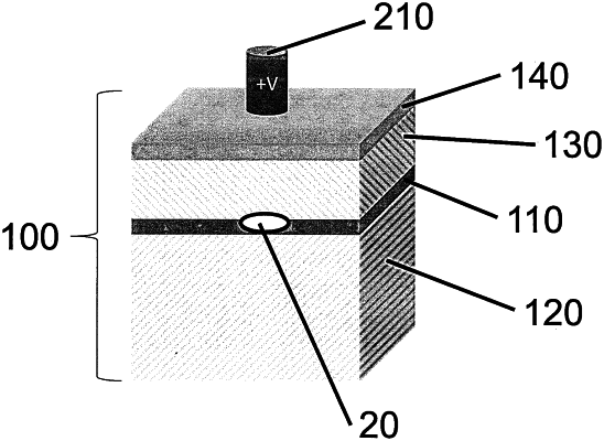
positioning at least one lead wire of a gate chip at a distance of less than 10 nm from a semiconductor heterostructure, the lead wire having a cross sectional width between 5 nm and 30 nm, the semiconductor heterostructure comprising a surface layer and at least one subsurface layer;
inducing a quantum dot in the semiconductor heterostructure, wherein an electrostatic potential is induced in the subsurface layer by applying a voltage between 0.01 V and 0.2 V to the lead wire such than an orbital energy for a given charge carrier of the induced quantum dot is larger than an energy level of an effective temperature bath;
loading a charge carrier into the subsurface layer;
detecting the charge carrier in the subsurface layer of the semiconductor heterostructure by:
emitting a radio-frequency pulse using a resonator having a Q factor of at least 103 coupled to the at least one lead wire of the gate chip;
detecting a reflected pulse of the emitted radio-frequency pulse; and
determining a phase shift of the reflected pulse relative to the emitted radio-frequency pulse; and
characterizing the quantum dot by measuring a valley splitting of the quantum dot.
|