US 11,810,966 B2
Semiconductor structure and method for fabricating the same
Haiyang Zhang, Shanghai (CN); and Panpan Liu, Shanghai (CN)
Assigned to Semiconductor Manufacturing International (Shanghai) Corporation, Shanghai (CN); and Semiconductor Manufacturing International (Beijing) Corporation, Beijing (CN)
Filed by Semiconductor Manufacturing International (Shanghai) Corporation, Shanghai (CN); and Semiconductor Manufacturing International (Beijing) Corporation, Beijing (CN)
Filed on Mar. 1, 2022, as Appl. No. 17/684,240.
Application 17/684,240 is a division of application No. 17/034,335, filed on Sep. 28, 2020, granted, now 11,302,803.
Claims priority of application No. 201911071524.9 (CN), filed on Nov. 5, 2019.
Prior Publication US 2022/0190138 A1, Jun. 16, 2022
Int. Cl. H01L 29/76 (2006.01); H01L 29/94 (2006.01); H01L 29/66 (2006.01); H01L 29/06 (2006.01); H01L 27/088 (2006.01); H01L 29/78 (2006.01); H01L 29/417 (2006.01)
CPC H01L 29/6681 (2013.01) [H01L 27/0886 (2013.01); H01L 29/0649 (2013.01); H01L 29/41791 (2013.01); H01L 29/785 (2013.01)] 10 Claims
OG exemplary drawing
 
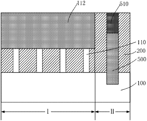
1. A semiconductor structure, comprising:
a substrate, including a first region and a second region;
a plurality of fins, formed on the first region of the substrate;
a first isolation structure, formed on the first region between adjacent fins and on the second region of the substrate;
a second isolation structure, formed in each fin and in the first isolation structure, over the first region of the substrate; and
a power rail, formed in the isolation structure and partially in the substrate of the second region, a top surface of the power rail being higher than a top surface of the plurality of fins.