| CPC H01L 29/45 (2013.01) [H01L 21/28518 (2013.01); H01L 21/823418 (2013.01); H01L 29/0847 (2013.01); H01L 29/41791 (2013.01); H01L 29/66795 (2013.01); H01L 29/7839 (2013.01); H01L 29/7851 (2013.01)] | 20 Claims |
|
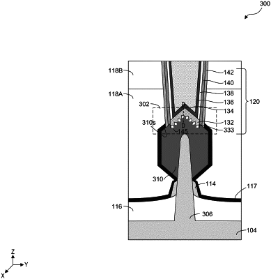
17. A semiconductor device, comprising:
a fin structure disposed on a substrate;
a source/drain (S/D) region disposed on the fin structure; and
a contact structure, comprising:
a first silicide layer, disposed on the S/D region, comprising:
a first metal,
a second metal different from the first metal, and
a faceted surface;
a second silicide layer comprising the second metal disposed on the first silicide layer, wherein the faceted surface is in contact with the second silicide layer; and
a contact plug disposed on the second silicide layer.
|