| CPC H01L 29/165 (2013.01) [H01L 21/28562 (2013.01); H01L 28/55 (2013.01); H01L 28/60 (2013.01); H01L 29/0688 (2013.01); H01L 28/40 (2013.01)] | 26 Claims |
|
1. A semiconductor device, comprising:
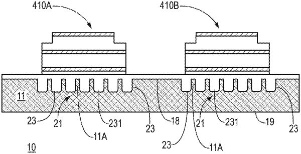
a work piece comprising a first material, a first side, a second side opposite to the first side, and a first coefficient of thermal expansion (first CTE);
recesses extending into the work piece from the first side and comprising a pattern;
a second material comprising a second CTE within the recesses and over the first material between the recesses; and
a third material comprising a third CTE over one of the second side or the second material;
wherein:
the third CTE and the second CTE are different than the first CTE.
|