| CPC H01L 29/0673 (2013.01) [H01L 21/0217 (2013.01); H01L 21/02236 (2013.01); H01L 21/02532 (2013.01); H01L 21/308 (2013.01); H01L 21/823412 (2013.01); H01L 21/823418 (2013.01); H01L 21/823431 (2013.01); H01L 27/0886 (2013.01); H01L 29/0847 (2013.01); H01L 29/1033 (2013.01); H01L 29/42392 (2013.01); H01L 29/6656 (2013.01); H01L 29/66545 (2013.01); H01L 29/7843 (2013.01); H01L 29/6659 (2013.01)] | 10 Claims |
|
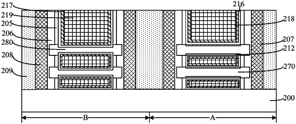
1. A semiconductor structure, comprising:
a semiconductor substrate having a first region and a second region, the first region being used to form peripheral devices, the second region being used to form core devices, and a voltage of the peripheral devices being greater than a voltage of the core devices;
first nanowires formed over the first region of the semiconductor substrate;
second nanowires with a diameter smaller than a diameter of the first nanowires formed over the second region of the semiconductor substrate;
a first gate layer formed around the first nanowires; and
a second gate layer formed around the second nanowires.
|