| CPC H01L 28/90 (2013.01) [H01L 21/31116 (2013.01); H01L 21/31144 (2013.01); H01L 28/92 (2013.01); H10B 12/033 (2023.02)] | 20 Claims |
|
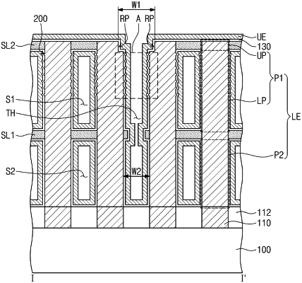
1. A semiconductor device, comprising:
a substrate;
a capacitor bottom electrode disposed over the substrate;
a first support layer disposed over the substrate and contacting a side surface of the capacitor bottom electrode;
a second support layer disposed over the first support layer and contacting the side surface of the capacitor bottom electrode;
a dielectric layer disposed on the capacitor bottom electrode, the first support layer and the second support layer; and
a capacitor top electrode disposed on the dielectric layer,
wherein the capacitor bottom electrode includes:
a first portion that is disposed between the first support layer and the second support layer, and disposed adjacent to the first support layer; and
a second portion that is disposed between the first support layer and the second support layer, and disposed adjacent to the second support layer,
wherein a side surface of the first portion of the capacitor bottom electrode is substantially flat, and
the second portion of the capacitor bottom electrode includes a plurality of protrusions that protrude from a side surface of the second portion of the capacitor bottom electrode.
|