| CPC H01L 27/153 (2013.01) [F21K 9/00 (2013.01); H01L 33/36 (2013.01); H01L 33/62 (2013.01)] | 15 Claims |
|
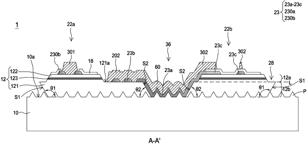
1. A light-emitting device, comprising:
a substrate, comprising an upper surface;
a first light-emitting unit and a second light-emitting unit adjacent to each other, formed on the upper surface, and wherein each of the first light-emitting unit and the second light-emitting unit comprises a lower semiconductor portion and an upper semiconductor portion;
wherein the lower semiconductor portion of the first light-emitting unit comprises:
a first upper surface not covered by the upper semiconductor portion of the first light-emitting unit;
a first side wall not facing the second light-emitting unit and adjacent to a periphery of the light-emitting device; and
a second side wall; and
a conductive structure, formed on the second side wall and electrically connecting the first light-emitting unit and the second light-emitting unit;
wherein the first side wall connects the first upper surface and the upper surface of the substrate, and an obtuse angle is formed between the first side wall and the upper surface of the substrate and an acute angle is formed between the second side wall and the upper surface of the substrate.
|