| CPC H01L 27/14647 (2013.01) [H01L 24/05 (2013.01); H01L 24/13 (2013.01); H01L 24/16 (2013.01); H01L 27/14612 (2013.01); H01L 27/14634 (2013.01); H01L 27/14636 (2013.01); H04N 13/204 (2018.05); G06T 7/521 (2017.01); G06T 2207/10024 (2013.01); G06T 2207/10028 (2013.01); H01L 24/14 (2013.01); H01L 2224/0401 (2013.01); H01L 2224/05554 (2013.01); H01L 2224/06131 (2013.01); H01L 2224/13013 (2013.01); H01L 2224/13016 (2013.01); H01L 2224/13147 (2013.01); H01L 2224/14131 (2013.01); H01L 2224/16014 (2013.01); H01L 2224/16145 (2013.01); H04N 25/75 (2023.01)] | 19 Claims |
|
1. A three-dimensional (3D) image sensor comprising:
a first substrate including an upper pixel array, a plurality of upper pixels of the upper pixel array are disposed in first rows and first columns of a first arrangement;
a second substrate including a lower pixel array including a plurality of lower pixels; and
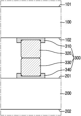
a bonding conductor array disposed between the first and second substrates, a plurality of bonding conductors of the bonding conductor array are disposed in second rows and second columns of a second arrangement and electrically connected between the upper pixel array and the lower pixel array,
wherein the second arrangement is inclined at an angle of 45° with respect to the first arrangement.
|