| CPC H01L 27/1463 (2013.01) [H01L 27/14623 (2013.01); H01L 27/14627 (2013.01); H01L 27/14636 (2013.01); H01L 27/14685 (2013.01)] | 20 Claims |
|
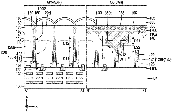
1. An image sensor comprising:
a substrate comprising a first side on which light is incident and a second side opposite to the first side;
a first separation pattern extending from the second side, the first separation pattern being interposed between a plurality of unit pixels in the substrate of a light-receiving region and a light-shielding region provided around the light-receiving region;
a second separation pattern extending from the first side and overlapping the first separation pattern, the second separation pattern being provided in the substrate of the light-receiving region; and
a contact film electrically connected to the first separation pattern, the contact film being provided in the substrate of the light-shielding region,
wherein a contact trench which extends from the first side is formed in the light-shielding region of the substrate and exposes the first separation pattern, and
the contact film fills at least a part of the contact trench.
|