US 11,810,935 B2
Imaging device, solid state image sensor, and electronic device
Atsushi Yamamoto, Kanagawa (JP)
Assigned to Sony Semiconductor Solutions Corporation, Kanagawa (JP)
Filed by Sony Semiconductor Solutions Corporation, Kanagawa (JP)
Filed on Mar. 16, 2022, as Appl. No. 17/696,800.
Application 17/696,800 is a continuation of application No. 16/616,164, granted, now 11,309,344, previously published as PCT/JP2018/018639, filed on May 15, 2018.
Claims priority of application No. 2017-105714 (JP), filed on May 29, 2017.
Prior Publication US 2022/0208821 A1, Jun. 30, 2022
Int. Cl. H01L 27/146 (2006.01); H04N 23/53 (2023.01); H04N 23/55 (2023.01)
CPC H01L 27/14625 (2013.01) [H01L 27/1462 (2013.01); H01L 27/14618 (2013.01); H01L 27/14623 (2013.01); H04N 23/53 (2023.01); H04N 23/55 (2023.01)] 11 Claims
OG exemplary drawing
 
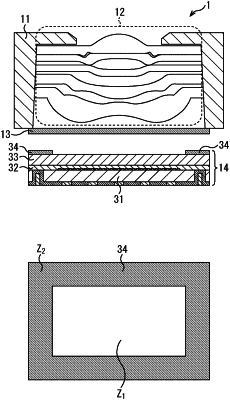
1. An integrated assembly for an imaging device comprising:
a pixel array;
an optical assembly comprising one or more transparent materials mounted with the pixel array in the integrated assembly; and
a light shield arranged to block light at a periphery of the integrated assembly, wherein a part of the light shield is disposed on at least one of the one or more transparent materials and wherein a width of a substrate including the pixel array is the same as a width of the optical assembly.