| CPC H01L 27/1244 (2013.01) [H01L 27/1259 (2013.01)] | 15 Claims |
|
1. A display substrate, comprising an Electric Test (ET) region, wherein
at least one testing pad and an insulation structure surrounding the testing pad are arranged in the ET region, and a distance between a surface of the insulation structure distal to a base substrate of the display substrate and the base substrate is not greater than a distance between a surface of the testing pad distal to the base substrate and the base substrate,
wherein the display substrate further comprises a display region, the ET region is arranged at periphery of the display region;
the testing pad is configured to be in physical contact with a pad of a flexible circuit board of the display substrate, to perform ET on the display substrate;
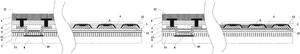
wherein the display substrate comprises an active layer, a gate insulation layer, a gate metal layer, an interlayer insulation layer, a first source/drain metal layer, a passivation layer, a first planarization layer, a second source/drain metal layer and a second planarization layer that are arranged sequentially in that order in a direction away from the base substrate, insulation film layers of the display substrate comprise the gate insulation layer, the interlayer insulation layer, the passivation layer, the first planarization layer and the second planarization layer, and a quantity of film layers of the insulation structure is smaller than a quantity of the insulation film layers of the display substrate;
wherein the insulation structure comprises the passivation layer and the first planarization layer, or the insulation structure comprises the passivation layer and the second planarization layer.
|